Blogs Directory

Saturday, January 25, 2014

SYSTEM VERILOG FOR DESIGN - PART 1


                 Verilog is a great language which is widely used in Industry but it had few limitations. Verilog is not helping verification engineers much. Also there were few ambiguities in designer code. Also the code is not precise. To over come these limitations verilog was enhanced to System verilog. SV is verification frendly which supports object oriented programming. It eliminated synthesis simulation misinterpretations and also made the code precise and easily maintainable. The objective of this post is to show the basic things which a designer need to know to code a design in SV.
                    First thing which differs SV from verilog is the enhanced data types. In hardware description language there is no such thing called data types. Hardware signal can be

      logic 1,
      logic 0,
      Unknown (X) and
      high impedance (Z).

In verilog the register and wire were used for the storing and connecting two storage units (flip flop). In system verilog the following data types can be used for RTL coding.
  • Logic - 4 stage variable and user defined size (can be used instead of reg and wire )
  • Enum - Variable which can have only user defined values
  • int - 32 bit , 2 stage integer variable. (can be used instead of integer)
  Enum is very useful variable which can store user defined data types. It helps especially while coding the state machines.

Example : 

          enum logic [2:0] 
              { START      = 3'b100,
                 PROCESS = 3'b010,
                 STOP        = 3'b001}
                state, next_state ;

The system verilog compiler would ensure that the values that are specified in the enum data type are unique. Hence the compiler would through an error if the values are same because of a typo like ,

          enum logic [2:0] 
              { START      = 3'b100,
                 PROCESS = 3'b010,
                 STOP        = 3'b100}
                state, next_state ;
           
But a traditional verilog code using the parameter would not show any compiler issues since the values assigned are for different variables.

parameter
         START      = 3'b100,
         PROCESS = 3'b010,
         STOP        = 3'b100;

struct :

Another very useful enhancement that system verilog brings is the structures. In RTL coding the structures can be used to bundle related signals together.

    struct {
        logic  Enable1;
        logic  [9:0] Data1;
        logic  Ack1; 
             } bus1;

We can assign values to the entire structure in a single assignment which reduces the number of lines in the rtl code.

    bus1 = `{1'b1, 10'b0101010101, 1'b1};

This is how we assign value to a member of struct.

   bus1.Ack1 = 1'b0 ;


typedef :

      SV also supports user defined data types using typedef. It can be used to define some complex data types which user might need to use multiple times easily. We need to know that we are creating a new data type using the typedef not the variable itself.

typedef logic [63:0] bus_64 ;

you could use the data type bus_64 that we created using typedef to create new variables of that kind.

bus_64 output;    (Here we have declared output as a 64 bit bus using typedef bus_64 which is created earlier)

packages :

    Often we might require to define the same variables or fuctions in multiple files which is duplication of same piece of code.  SV has introduced packages that we could use it to simplify the re declaration and maintain consistency in the code.

  package common_def {
     typedef logic [31:0] bus_64;
     enum logic [2:0] 
              { START      = 3'b100,
                 PROCESS = 3'b010,
                 STOP        = 3'b001
              } state, next_state ;
       struct {
        logic  Enable1;
        logic  [9:0] Data1;
        logic  Ack1; 
                } bus1;         
  endpackage

The package common_def can be imported to any system verilog file using import command and there you get all the definitions.

  import common_def::*;

  module control ();
  bus_64 system_bus;
  ...
  endmodule

array :  


  SV also supports multi dimensional arrays which are synthesize-able. The advantages is we could address the whole bunch of bits together in one assignment.

  logic [31:0] data ; (Normal verilog 32 bit variable)

  logic [1:0] [3:0] [3:0] data ; (Multi dimentional 32 bit variable)

  The advantage is we could assign values in different ways,

   assign data [1][1][1] = 1'b1;
   assign data [1][1] = 4'hF;

Lets discuss about interfaces , procedural blocks and other enhancements in next part.

Wednesday, January 22, 2014

ASIC SYNTHESIS - PART 1 (INTRODUCTION)


             Synthesis is a process of converting higher abstraction level (HDL Coding) into lower abstraction level (Gate Netlist). This process is termed as synthesis because it is the process in which we combine the various basic gates into a full chip netlist as described in the HDL (Hardware Description Language). It also involves making the design adhere to the requirements like timing, area and power. Nowadays the size and complexity of the chips have increased multi-fold. Hence we cannot do it manually. Also the purpose of higher abstraction that HDL gives to designers is of no use if we have to do the synthesize manually. There are couple of tools available from the EDA companies which does a good job for us. 
  
                 In order for you to become an expert in synthesis you have to have first know three things,


  • Overall flow - You need to understand the very existence of the synthesis in the IC design flow. Synthesis in itself involves many stages. you need to know what are they and why are they important. 
  • Tool behavior - Tools help us a lot in automating the stuff. We have to know how we can best benefit from the tool available to us. A good command over the tool that we use saves us a lot of time in debug and helps us to achieve our goals sooner.                                                                     
  • Hands On - Unless you practice all that you have learnt you will never become an expert. Without hands on you even forget the concepts and tool commands. You can easily develop an synthesis flow for yourself for practice.                            
               But am not going to cover the three things separately. What i will try to show is how a real time synthesis is done, what are the inputs, what are the outputs, what are the things we have to take care, Is the quality of the output met out requirements etc. Okay lets get started. Before you start any thing you have to make sure you have all the inputs that are required for the job. In Synthesis most of the quality that you get is based on the quality and completeness of the inputs.
               What i have decided is to code a simple design by hand in system verilog and explain every step until the scan netlist is generated with good quality. By following these series of posts you will be able to 
  1. Understand basics of System Verilog for RTL coding.
  2. Setup synthesis environment.
  3. Perform power aware synthesis using Design Compiler Topo.
  4. Know Scan techniques and flow.
                Assumption is you know 

     1. Basics of Verilog.
     2. Know where synthesis stands in the IC design flow.
     3. Know why scan is required.


Monday, January 13, 2014

System on a chip (SoC)

       
              System on a chip concept is very important for the evolution of the future devices. Earlier each function of the system is implemented in separate chips. The evolution of personal computers is an example for the system on chip concept. In earlier days the processor was a separate chip and all other functions like graphics, IO's, WLAN etc are implemented separate chips. But nowadays the duopoly companies Intel and AMD is in a race to integrate as many functions into a single chip thereby simplifying the system cost and complexity. Current SOC's of AMD integrate CPU, GPU and IO in a single chip. Qualcomm is the preferred supplier of chipsets for the high end smart phones because it of its integration of the communication IP in its application processors. Intel has integrated an on-chip voltage regulator. Integration like this make Original Equipment Manufactures (OEM) to come up with new designs. 
                 Though the SOC concept provides lot of advantages it introduces a lot of complexities for the chip manufacturers. Various IPs need to be made work in same process nodes, manage power dissipation etc. SOCs indeed reduce the overall power consumption of the system. Chip manufacturing technology is also one of the contributor for the SOC concept. Every two years the number of transistors in a die of same size would double itself. This tempts the chip manufacturers to add more and more features into their chip sets there by differentiating them-self from their competitors. The concept of integrated graphics in PC microprocessor chips is a clear example stating this trend. Advancements in the manufacturing technology which i witnessed from 65nm to 20nm has made chip manufactures rethink about their architectures. Many SOCs nowadays have multiple cores for compute rather that one core in earlier days. This is in one way of taking advantage of the silicon down scaling. 
                    The picture here bellow shows the Nvdia's Tegra SoC for tablets. What we could see here is apart from the ARM processor it has got a image processor, GeForce Graphics processor unit and other bunch of connectivity IPs. This we call it a system on a chip. Gradually every bit of the motherboard is pulled into the integrated circuit thereby making the devices miniaturization and improve the performance.

                            
                                                   Pic : Tegra SOC . Courtesy : Nvdia                      

                       The ultimate beneficiaries of the system on a chip concept are the end consumers. The toatl cost of the device comes down exponentially with highly integrated SOCs. Also the reliability and the performance of the device is greatly improved. Power consumption of the system can be reduced substantially by integrating more and more of the functions into the single SOC. The SOC concept should not be confused with SIP (System in Package). SIP has many integrated circuits kept in a single packaging. usually the integrated circuits are stacked vertically. 3D packaging techniques have been developed to stack many integrated circuits one above the other. SOC concept have more advantages than compared to SIPs.
                         SOC concept is the future of integrated circuits. Ultimately all the functionality will be fabricated in a single silicon chip giving rise to a new era of electronic devises. Soon we might see embedded able chips that can offset human disabilities like vision, sense etc. 

Friday, October 11, 2013

Splitting a line into multiple lines and vice versa

This is the most common situation that we encounter in our work flows. I work in SOC team and there by need to do lot of text manipulations. Here i learnt that splitting a line into multiple lines and multiple lines into a single line using the method bellow.

Example 1:   (Text)

America
Africa
India
Germany

Use this command in the command mode of vim :%s/\n/ / 

The output would be like this :
 America Africa India Germany

Example 2: (Text)

America Africa India Germany

Use this command in the command mode of vim to split the line into multiple lines :%s/ /^M/g
% -> works on all the lines in the file
s -> substitute command
/ -> command divider
^M -> we get this by pressing <Ctrl>V followed by Enter.
g -> works on multiple occurrence of the pattern in the line.

Wednesday, September 18, 2013

Power Dissipation basics


                    The three main goals in chip design are timing, area and power. But because of the raise in mobile phones and smartphones the battery life of handheld devices became a major selling point in the market rather than the speed of the processor and area. Hence an architect of the chip must design the chip with minimum power dissipation possible. There are many techniques for reducing the total power and peak power dissipation. Before that we need to understand the cause for the power dissipation and the parameters involved in it. Based on the parameters that contribute to the power dissipation we might find some techniques that can be employed to reduce the power. 


Sunday, August 4, 2013

Spread Spectrum Clocking to reduce EMI


                      Before we jump into the technique of spread spectrum clocking, let us understand why it it been used so widely. All the electronic devices emits Electro-magnetic radiation. This electro magnetic radiation can interfere with the surrounding systems like other on-board systems, radio, TV etc. Because of this governments across the world have been regulating the amount of EMI (Electro Magnetic Interference) an electronic system can emit. EMI can interrupt, degrade or reduce the performance of the system. These can cause simple degradation of the data to the total loss of the data. 
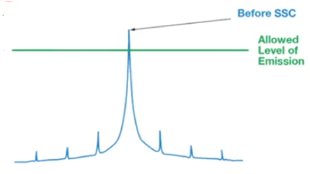
                    Electro magnetic radiation in digital systems can in many cases exceed the regulatory guidance because of the periodic nature of the signals. Clocks in the digital systems are periodic. It means they have a fixed frequency. Because of the fixed frequency, the radiated power has peak values. This due to the harmonics. Continuous repeated radiations builds up harmonics that amplifies the radiated power which can cause severe noise interference to the surrounding systems. Hence the solution we can think of is to avoid the periodicity (fixed frequency). You might wonder how can we implement this. Nowadays SSC (Spread Spectrum Clocking) has become widely used method to reduce the peak EMI power. 

In the picture above the radiated power concentrates in one particular frequency. Hence we can see that the emitted power has peak value which very well exceeds the allowed levels of emission. In order to avoid this peak emission powers, spread spectrum clocking allows us to distribute the clock frequency over a range of frequencies there by we could avoid harmonics and therefore peak power emissions. 
               There are 4 important parameters in the SSC, they are :
  • Modulation index : amount of frequency (or spread) as a relative percentage of the input or the carrier frequency.
      Example : 1% spread means an input/carrier frequency of 100MHz is spreading from 99MHz to 101MHz.
  • Modulation frequency : the rate at which the input or carrier frequency will change between the min and max range.
       Example : with 1% spread on input frequency of 100MHz, modulation frequency says the rate in which the frequency changes between 99 to 101MHz.
  • Modulation profile : how the clock frequency is modulated between min and max frequency range.
  • Spread type :  there are two types of spreads down spread or the center spread.

  1.  down spread : the spread range is bellow the input frequency. from 98MHz to 100MHz for -2% down spread for above example.
  2. center spread : the spread range distributes evenly with center as input frequency. 99MHz to 101MHz for 1% center spread.

How can we implement SSC ?  

Thursday, July 11, 2013

Process Corners... What and Why ?

                    Semiconductor manufacturing is very complex process with many stages. The complexity lies in the geometries that we are building chips. Technology is developing at a faster phase because of the market competition and demand. The transition from 90nm to 28nm happened within a decade. Wafer size grown from 200mm to 450mm. As the foundry vendors try to move on to the smaller geometries, the design companies need to verify the chip design thoroughly for all possible variability in the manufacturing process. Variability plays a major role in determining how best is the foundry manufacturing process.
                 The ideal goal is to produce every chip exactly the same. But it is not possible since not all the factors can be controlled to be in an ideal way. The conditions in which the chips are fabricated causes these variations in the properties. The heart of the foundry is the clean room. The temperature, humidity and even the vibrations are to be controlled.
                 Some of the process parameters like implant dose, channel length, threshold voltage can vary in some degrees. Hence the behavior of the transistors vary accordingly. What manufactures do is they make corner lots. Corner lots means they bundle the wafers based on these process parameters worst, typical and best. The characterization team couple temperature, voltage and frequency of operation with these process parameters and plot the responses on a plot called shmoo plot. Bellow picture shows the shmoo plot for a variable voltage. X in the bellow picture indicate positive response and "." a negative one.


                     Based on these plots we come to know the boundary beyond which the device will fail for the various combinations of these parameters. Actually these process variations arise due to many reasons such as the temperature and humidity in which the wafers are made, the precision of the manufacturing machines in which it can fabricate the dies. After the characterization is done, normally the characteristic responses of the devices are modeled  as NLDM or CCS libraries for worst typical and best conditions of the devices. They are normally named using a two letter terminology like SS, TT and FF etc. They mean fast, slow and typical carrier mobilities of the devices. Wonder why there are two characters ? First one is for NMOS and second is for PMOS. TT does not actually represent any relative process corner effect but its just the nominal corner over which the process technology would have most probable outcome. So we always want to test our devices in the extreme process variations to ensure that there is always a good margin for a better yield. Therefore the combination of process corners would be SS, FF, TT, SF and FS. SS, TT and FF corners are the even corners where we can expect strong correlation in the PMOS and NMOS behavior since both would be either slow or faster. But SF and FS corners are called as Skewed corners in which the delay exhibited by the PMOS and NMOS are different leading to output signal to have different slews on rise and fall edges. PMOS controls the rise transitions and NMOS controls the fall transitions of the output signal. If we have both of them operating at the same way the output transitions rise or fall would have same slew. But if they are different the transition will be different. We usually do not consider SF and FS corners because they get covered in the SS and FF corner.

                      SS - Slow NMOS and Slow PMOS
                      SF - Slow NMOS and Fast PMOS
                      FS - Fast NMOS and Slow PMOS
                      TT - Typical NMOS and Typical PMOS
                      FF - Fast NMOS and Fast PMOS

                     Now that we have understood the differences due to the process variations, the device characteristics also varies due to the voltage and temperature. We need to couple the voltage and temperature with the process corners to obtain the actual possible corners. Before that we have to understand the device characteristics for various voltages and temperature.
                            Semiconductor devices operate better with better voltage. Hence delay decreases with increase in the voltage. For a slow corner we would choose min voltage and for a fast corner we would choose max voltage. These min and max voltages are based on the voltage specifications of the product.

                       Max Voltage -> Less Delay
                       Min Voltage -> More Delay

                               When it comes to temperature, we need to be little cautious. In the technologies above 90nm delay increases as temperature increases. This is due to the fact that as the temperature increases the electrons collides more often that disrupts the stream line flow which makes the current flow. This effect is called lattice scattering. The lattice vibrations due to high temperature scatters the electrons. As the geometries scales smaller and smaller the effect of temperature on delay varies at lower temperature. At lower temperature the impurity scattering becomes dominant where as the thermal motion of the electron is slower. As the electrons moves slower they get easily scattered by the impurity ions. This effect becomes more dominant at lower voltages. Hence before we could decide on the corner for implementations and sign off we need to do a temperature inversion analysis.

What is temperature inversion analysis ?

              As we have seen that the delay of the cells cannot be scaled with the temperature we need to do a temperature inversion analysis to first understand the corners for which the cells in the library has more delay. This is very important since we may choose a single worst corner for implementation to avoid run times issues due to multi corner synthesize. The method to do this temperature inversion analysis is,

  1. Select one cell for each type from the library. For example, and, or, exor, clock buffer, flop etc
  2. Load the spice model of the cell into a spice simulation tool.
  3. Note the delay of the cell using 50% to 50% transition from input to output and transition using 30% to 70% for various combination of input slew and load. 
  4. Repeat step 3 and 4 for min temperature and max temperature using SS process corner and min voltage.
  5. Form a two dimensional table for each cell type with slew and load in X and Y axis. Make such table for min and max temperature.
  6. From the tables high light the max delay values. 
By analyzing the max delay values from each table we can identify the process, voltage and temperature (min/max) combination which produces the max cell delays. From that we can choose the worst corner for implementation. In case if the cell delay is more only for a few combinations of input slew and load, then we may have to choose temperature showing max delay for implementation and do a signoff check in both min and max temperature. This is called Partial temperature inversion. If you notice cell delays are maximum in all tables for min temperature, then we can safely avoid max temperature corner. One common trend is the temperature inversion becomes more dominant at min voltages. So if you are choosing min temperature then most probable there should be min voltage along with that.         
                    
             Similar to the different corners that exist to the PMOS and NMOS, there are different corners for interconnect as well.

Interconnect Corners :
              Interconnects also experience some variations due to the manufacturing process technology. The width, thickness of the metal traces, dielectric constant of the spacing and width of the spacing can vary. Because of this the resistance and capacitance of the metal traces vary which ultimately has an impact on the delay of the interconnect. See the picture bellow to better understand the interconnect process variation effects on the delay. 


       The picture above is how the metal traces appear when you cut the chip into two pieces and look into the cut portion. Adjacent metal layers are oriented at 90 degree angles. Between the metal traces is the dielectric material (like Si02). Because of the variation in the height and width of the metal traces the capacitance and resistance varies. 

1. Resistance increases if  
  • Width decreases.
  • Temperature increases.

2. Capacitance increases if 
  • Spacing between the metal traces decreases.
  • Height increases.
As the technology nodes gets smaller and smaller the above mentioned factors fuels increase in resistance and capacitance. As we know delay is calculated for an interconnect by the formula,

                                  Delay = R*C

Today there are 5 corners that are being used for interconnects. They are,

  • C Best : In this the Capacitance of the interconnect is minimum. Capacitance becomes minimum when there is minimum Height, Width of the metal trace, hence resistance increases. 
  • C Worst : In this the Capacitance of the interconnect is maximum. Capacitance becomes maximum when there is maximum Height, Width of the metal trace hence resistance decreases.
  • RC Best : In this the product of the RC is minimum, in other words the interconnect delay is minimum. We cannot exactly predict the R/C contributions for the delay.
  • RC Worst : In this the product of the RC is maximum, in other words the interconnect delay is maximum. We cannot exactly predict the R/C contributions for the delay.
  • Typical : This is the corner in which the interconnects are fabricated mostly. The delay is typical.
While selecting the corners for the timing analysis, temperature needs to be considered. At low temperature the metal exhibits low resistance but ah high temperature  its quite opposite. Hence if you analyze the timing of a net at min and max temperature, it will differ a lot.  Hence we need to do an analysis of the net delays based on the above mentioned corners and parameters on our technology library to know what combinations gives worst / best delays.